- 您现在的位置:买卖IC网 > Sheet目录369 > W949D2CBJX5E (Winbond Electronics)IC LPDDR SDRAM 512MBIT 90VFBGA
�� �
�
�W949D6CB� /� W949D2CB�
�512Mb� Mobile� LPDDR�
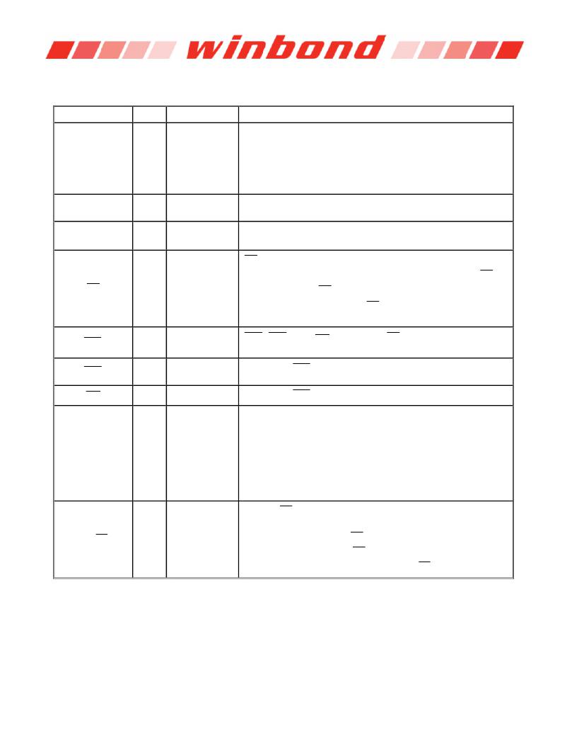
�4.� PIN� DESCRIPTION�
�4.1� Signal� Descriptions�
�SIGNAL� NAME�
�TYPE�
�FUNCTION�
�DESCRIPTION�
�Provide� the� row� address� for� ACTIVE� commands,� and� the� column�
�address� and� AUTO� PRECHARGE� bit� for� READ/WRITE�
�A� [n� :� 0]�
�Input�
�Address�
�commands,� to� select� one� location� out� of� the� memory� array� in� the�
�respective� bank.� The� address� inputs� also� provide� the� opcode�
�during� a� MODE� REGISTER� SET� command.�
�A10� is� used� for� Auto� Pre-charge� Select.�
�BA0,� BA1�
�DQ0~DQ15� (×16)�
�DQ0~DQ31 (×32)�
�Input�
�I/O�
�Bank� Select�
�Data� Input/�
�Output�
�Define� to� which� bank� an� ACTIVE,� READ,� WRITE� or�
�PRECHARGE� command� is� being� applied.�
�Data� bus:� Input� /� Output.�
�CS� enables� (registered� LOW)� and� disables� (registered� HIGH)�
�the� command� decoder.� All� commands� are� masked� when� CS� is�
�CS�
�Input�
�Chip� Select�
�registered� HIGH.� CS� provides� for� external� bank� selection� on�
�systems� with� multiple� banks.� CS� is� considered� part� of� the�
�command� code.�
�RAS�
�Input�
�Row� Address�
�Strobe�
�RAS� ,� CAS� and� WE� (along� with� CS� )� define� the� command�
�being� entered.�
�CAS�
�Input�
�Column� Address� Referred� to� RAS�
�Strobe�
�WE�
�Input�
�Write� Enable�
�Referred� to� RAS�
�Input� Data� Mask:� DM� is� an� input� mask� signal� for� write� data.� Input�
�data� is� masked� when� DM� is� sampled� HIGH� along� with� that� input�
�data� during� a� WRITE� access.� DM� is� sampled� on� both� edges� of�
�UDM� /� LDM(x16);�
�DM0� to� DM3� (x32)�
�Input�
�Input� Mask�
�DQS.� Although� DM� pins� are� input-only,� the� DM� loading� matches�
�the� DQ� and� DQS� loading.�
�x16:� LDM:� DQ0� -� DQ7,� UDM:� DQ8� –� DQ15�
�x32:� DM0:� DQ0� -� DQ7,� DM1:� DQ8� –� DQ15,�
�DM2:� DQ16� –� DQ23,� DM3:� DQ24� –� DQ31�
�CK� and� CK� are� differential� clock� inputs.� All� address� and� control�
�input� signals� are� sampled� on� the� crossing� of� the� positive� edge� of�
�CK� /� CK�
�Input�
�Clock� Inputs�
�CK� and� negative� edge� of� CK� .Input� and� output� data� is� referenced�
�to� the� crossing� of� CK� and� CK� (both� directions� of� crossing).�
�Internal� clock� signals� are� derived� from� CK/� CK� .�
�Publication� Release� Date:� Sep,� 21,� 2011�
�-6-�
�Revision� A01-007�
�发布紧急采购,3分钟左右您将得到回复。
相关PDF资料
W971GG6JB25I
IC DDR2 SDRAM 1GBIT 84WBGA
W971GG8JB-25
IC DDR2 SDRAM 1GBIT 60WBGA
W9725G6IB-25
IC DDR2-800 SDRAM 256MB 84-WBGA
W9725G6JB25I
IC DDR2 SDRAM 256MBIT 84WBGA
W9725G6KB-25I
IC DDR2 SDRAM 256MBIT 84WBGA
W972GG6JB-3I
IC DDR2 SDRAM 2GBITS 84WBGA
W9751G6IB-25
IC DDR2-800 SDRAM 512MB 84-WBGA
W9751G6KB-25
IC DDR2 SDRAM 512MBIT 84WBGA
相关代理商/技术参数
W949D2CBJX5ETR
制造商:Winbond Electronics Corp 功能描述:512M MDDR, X32, 200MHZ
W949D2CBJX5I
制造商:Winbond Electronics Corp 功能描述:DRAM Chip Mobile LPDDR SDRAM 512M-Bit 16Mx32 1.8V 90-Pin VFBGA
W949D2CBJX5I TR
制造商:Winbond Electronics Corp 功能描述:512M MDDR, X32, 200MHZ, INDUST
W949D2CBJX6E
制造商:Winbond Electronics Corp 功能描述:DRAM Chip Mobile LPDDR SDRAM 512M-Bit 16Mx32 1.8V 90-Pin VFBGA
W949D2CBJX6ETR
制造商:Winbond Electronics Corp 功能描述:512M MDDR, X32, 166MHZ, 65NM
W949D2CBJX6G
制造商:WINBOND 制造商全称:Winbond 功能描述:512Mb Mobile LPDDR
W949D2KBJX5E
制造商:Winbond Electronics Corp 功能描述:512M MDDR, X32, 200MHZ 制造商:Winbond Electronics Corp 功能描述:IC MEMORY
W949D2KBJX5I
制造商:Winbond Electronics Corp 功能描述:IC MEMORY